Für viele stellt sich eigentlich gar nicht mehr die Frage ob Apple mit dem iPhone 5 wieder einen „Rekord im Abspecken“ hinlegen wird. Es soll, so die Erwartungen und auch das eine oder andere Gerücht, noch dünner werden als das 9,3 mm dicke iPhone 4S. Kameramodule können mit solchen Reduktionen aber nur schwer mithalten.
Auftritt für Sony: Der Sensor-Spezialist präsentiert einen völlig neuen „back-illuminated CMOS image Sensor“, der für ein noch dünneres iPhone 5 wie gerufen kommt.
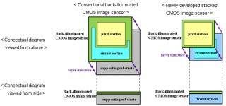
This image sensor layers the pixel section containing formations of back-illuminated structure pixels onto chips containing the circuit section for signal processing, which is in place of supporting substrates for conventional back-illuminated CMOS image sensors. This structure achieves further enhancement in image quality, superior functionalities and a more compact size that will lead to enhanced camera evolution.
Vorteile des RGBW-kodierenden Sensors (zu Rot, Grün und Blau kommt ein Weiß-Sensor hinzu) sind bessere Bildverhältnisse, besonders in dunklen Situationen, und schärfere Videos mit einem breiteren Lichtspektrum (sprich: HDR).
httpvh://www.youtube.com/watch?v=fM2xYCcbV5U
Natürlich ist noch nicht bekannt, ob Apple einen solchen Sensor in der nächsten iPhone-Generation verwenden will. Es wäre aber nicht überraschend, wenn der Tech-Gigant wieder einmal zur besten Technik auf dem Markt greifen würde, um seinem iPhone weiterhin die entscheidenden Vorteile gegenüber der Konkurrenz zu geben.
Die vollständige Presseaussendung von Sony:
Sony Develops Next-generation Back-Illuminated CMOS Image Sensor
which Embodies the Continuous Evolution of the Camera
– Expanding Shooting Enjoyment and Advanced Functionality of Smartphones and Other Devices –
Tokyo, Japan – January 23, 2012 – Sony Corporation (“Sony”) today announced that it has developed a new next-generation back-illuminated CMOS image sensor which embodies the continuous evolution of the camera. This image sensor layers the pixel section containing formations of back-illuminated structure pixels onto chips containing the circuit section for signal processing, which is in place of supporting substrates for conventional back-illuminated CMOS image sensors. This structure achieves further enhancement in image quality, superior functionalities and a more compact size that will lead to enhanced camera evolution.
Hereafter, Sony will position it as the next generation back-illuminated CMOS image sensors, and unwaveringly strive to further develop this image sensor and expand its product lineup, thereby contributing to the further development of user-friendly cameras and to shooting enjoyment.
Features of stacked CMOS image sensorLarge-scale signal processing circuits required for higher image quality and better functionality are built-in
More compact image sensor chip size
Even higher image quality of the pixel section by adopting manufacturing processes specialized for superior image quality
Faster speeds and lower power consumption by adopting the leading process for the circuit sectionBackground of development
The popularization of smartphones and other devices in recent years has been accompanied by an increasingly diverse use of camera functionality. This has brought heightened demand for more sophisticated cameras, to ensure adaptability to a wider range of scenes and Sony developed this stacked CMOS image sensor to meet such demand. In addition to the higher pixel numbers, superior image quality and faster speeds which conventional image sensors pursued, the newly-developed image sensors further achieve more highly-advanced functionalities and a more compact size, thus paving the way for enhanced camera evolution.
As the first step towards the commercialization of its new CMOS image sensors, Sony has developed a model with built-in signal processing functionality, an element that usually requires external embedment. Samples will be shipped from March, 2012. Accordingly, models have been developed with Sony's unique “RGBW Coding” function, which facilitates low noise, high quality image capture even in low light condition, and the proprietary “HDR (High Dynamic Range) Movie” function, which achieves brilliant color even when taking pictures against bright light.
About stacked CMOS image sensors
Conventional CMOS image sensors mount the pixel section and analog logic circuit on top of the same chip, which require numerous constraints when wishing to mount the large-scale circuits such as measures to counter the circuit scale and chip size, measures to suppress noise caused by the layout of the pixel and circuit sections, and optimizing the characteristics of pixels and circuit transistors.
Sony has succeeded in establishing a structure that layers the pixel section containing formations of back-illuminated structure pixels over the chip affixed with mounted circuits for signal processing, which is in place of supporting substrates used for conventional back-illuminated CMOS image sensors. By this stacked structure, large-scale circuits can now be mounted keeping small chip size. Furthermore, as the pixel section and circuit section are formed as independent chips, a manufacturing process can be adopted, enabling the pixel section to be specialized for higher image quality while the circuit section can be specialized for higher functionality, thus simultaneously achieving higher image quality, superior functionality and a more compact size. In addition, faster signal processing and lower power consumption can also be achieved through the use of leading process for the chip containing the circuits.
1 Kommentar
Kommentare sind geschlossen.


richtig geil, im video sieht man extrem den unterschied!!!!